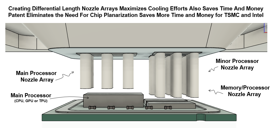
Differential Length Nozzle Arrays
Historically, microprocessors have been thinned and planarized so that every die in a package can mate uniformly to a common heat spreader through a TIM layer. That requirement made sense when a package contained a single monolithic die, or at most a small number of similar dies.
With the transition to 2.5D and 3D architectures—GPUs surrounded by HBM stacks, chiplets of varying function and material, interposers, and heterogeneous dies—the requirement that every surface be mechanically forced into the same plane has become increasingly burdensome. Each die type has different thickness tolerances, materials, coefficients of thermal expansion, and yield sensitivities. Planarization is no longer just a finishing step; it has become a costly, yield-impacting bottleneck.
Differential Length Nozzle Arrays
Maximizing Cooling Performance While Eliminating Chip Planarization Costs
MezzoFluidics’ patent pending Differential Length Nozzle Array architecture eliminates the need to mechanically force all dies to the same height. Instead of flattening silicon to satisfy a cooling interface, the cooling interface adapts to the silicon.
Each nozzle-impingement jet is fabricated at a specific, controlled length. The array is therefore “topography-aware.” In a package containing a GPU die, multiple HBM stacks, and surrounding chiplets—each at slightly different elevations—the nozzles are matched to maintain a consistent standoff distance above every heat-generating surface. Cooling performance becomes uniform without requiring the dies themselves to be made uniform.
This directly attacks the cost and complexity of today’s planarization pipeline:
Back-grinding (die thinning)
Fine grinding
Chemical Mechanical Polishing (CMP)
Planarization across heterogeneous dies
Packaging under a common lid
These steps exist primarily to ensure that a rigid heat spreader can make even contact across all chips. Differential Length Nozzle Arrays remove that mechanical dependency. The MezzoFluidics fixture does not require every die to be co-planar—it only requires that each nozzle terminate at the correct distance from its target surface.
The implications are profound:
Planarization becomes optional rather than mandatory.
Yield losses associated with over-thinning, microcracking, and CMP damage are reduced.
Packaging complexity in multi-die modules is lowered.
Time-to-package shortens by eliminating or relaxing CMP and die-thinning tolerances.
Foundries and OSATs (including TSMC, Intel, and their partners) avoid one of the most expensive and yield-sensitive steps in advanced packaging.
From a thermal perspective, performance improves simultaneously:
Each die receives optimized impingement geometry.
Nozzles can be positioned closer to high-power dies and slightly farther from lower-power regions.
Hotspots on GPUs and HBM stacks are addressed individually rather than averaged through a heat spreader.
Cooling efficiency increases while pressure and flow requirements decrease.
In effect, MezzoFluidics replaces mechanical conformity with fluidic conformity. Instead of grinding silicon to meet a flat metal lid, the cooling architecture conforms to the real geometry of the package. The result is higher thermal performance, lower system pressure, reduced manufacturing cost, improved yield, and a packaging flow that scales naturally with the heterogeneous, multi-die future of high-performance computing.
A note about OSATs:
OSATs are Outsourced Semiconductor Assembly and Test providers.
They are the companies that take finished wafers from foundries (like TSMC, Intel Foundry, Samsung Foundry) and perform:
Die singulation (cutting wafers into individual chips)
Advanced packaging (2.5D, 3D, chiplets, HBM integration, interposers)
Attaching dies to substrates
Applying heat spreaders or lids
Final electrical test and burn-in
Qualification for shipment
In today’s ecosystem:
Foundries build the transistors.
OSATs build the package that turns dies into a usable processor.
Major OSATs include:
ASE Group (Advanced Semiconductor Engineering);
Amkor Technology;
JCET Group;
SPIL (Siliconware Precision Industries);
Powertech Technology Inc. (PTI);
Tongfu Microelectronics;
ChipMOS;
Huatian Technology;
These firms are deeply involved in:
CoWoS, InFO, EMIB, Foveros-style packaging;
HBM integration around GPUs;
Multi-chip modules (MCM);
System-in-Package (SiP) designs;
Therefore when MezzoFluidics reduces cost and complexity for TSMC, Intel, and OSATs, it means:
Foundries can relax die thickness tolerances;
OSATs can simplify or skip aggressive CMP and planarization;
Advanced packages no longer need every die forced into the same plane;
Yield improves, cycle time drops, and packaging risk decreases;
Foveros is Intel’s trademarked technology for true 3D chip stacking—it is a vertical integration packaging method rather than a side-by-side (2.5D) approach.
Instead of placing multiple dies next to each other on an interposer, Foveros allows:
One die to be stacked directly on top of another
Electrical connections made through micro-bumps and through-silicon vias (TSVs)
Very short interconnect paths between logic, memory, and I/O layers
In practical terms, Foveros lets Intel build processors like a layered cake:
A base “active interposer” die handles power delivery and I/O
One or more compute dies (CPU, GPU, accelerators) are stacked above it
Additional tiles (AI blocks, cache, memory interfaces) can be added as layers
This architecture enables:
Higher transistor density without shrinking a single monolithic die;
Mixing different process nodes (e.g., 5 nm logic on top of 22 nm I/O);
Better performance per watt;
Smaller packages with more functionality;
From a thermal perspective, Foveros makes heat removal far more difficult:
Power-dense dies are no longer all on the top surface
Heat must travel through other active layers
Hotspots can form in buried silicon
That is precisely where MezzoFluidics’ technology becomes strategically important:
Differential Length Nozzle Arrays can be tailored to stacked die topography
Direct impingement can target the most power-dense regions
Eliminating heat spreaders and TIM layers reduces vertical thermal resistance
Lower pressure operation reduces mechanical stress on stacked structures
In short:
Foveros represents the future of high-performance packaging.
MezzoFluidics represents the future of cooling that future.
MezzoFluidics' Differential Length Nozzle Array is therefore not just a cooling innovation—it is a packaging workflow innovation that directly benefits the OSAT layer of the semiconductor industry.